


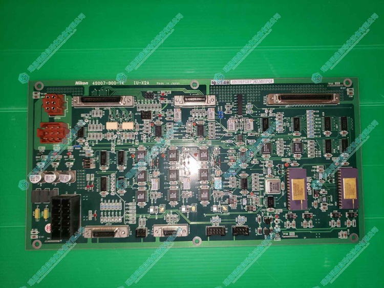
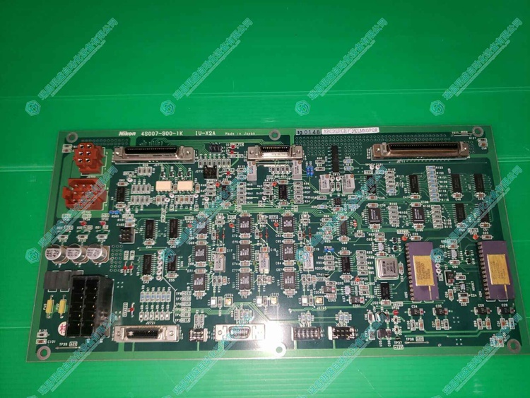
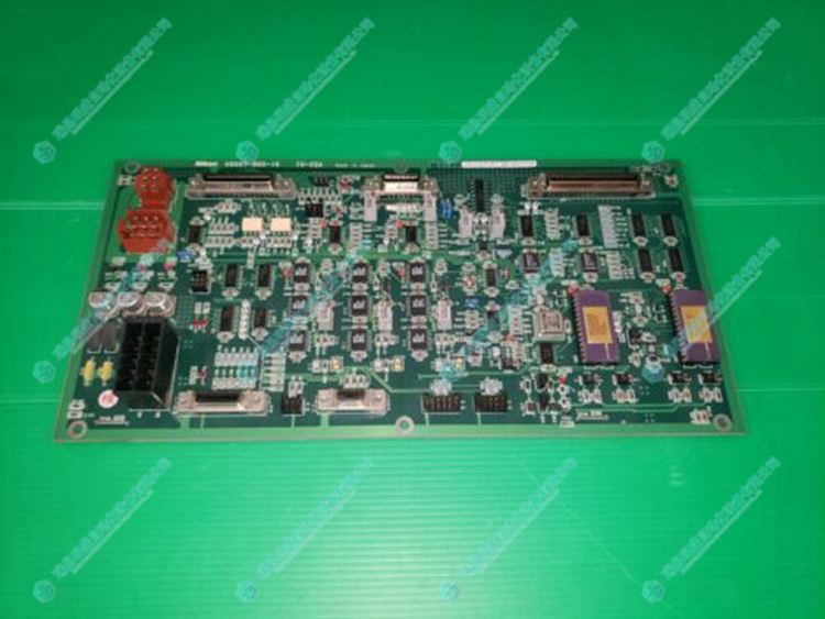
Nikon 4S007-900-1K 印刷电路板
1.产 品 资 料 介 绍:
中文资料:
Nikon 4S007-900-1K印刷电路板(Printed Circuit Board,PCB)是一种用于支持和连接电子组件的基础设施。PCB 提供了一种机械支持和电气连接的方式,使得电子设备的组装和连接变得更加容易和可靠。以下是 PCB 的一些基本信息:
材料: Nikon 4S007-900-1KPCB 通常由绝缘材料制成,如玻璃纤维增强的环氧树脂(FR-4)是常见的选择。其他材料如金属基板(铝或铜)也可以用于特定应用。
层次结构: Nikon 4S007-900-1KPCB 通常具有多层结构,其中导电层和绝缘层交替叠加。内部导线通常通过孔连接,这些孔称为“通孔”(Via)。
导线: 金属箔,通常是铜,用于形成电路中的导线。这些导线在 PCB 表面上形成复杂的图案,连接电子元件。
焊盘: 用于焊接电子组件引脚的金属区域。它们通过印刷或镀金属来增强电气连接。
印刷技术: Nikon 4S007-900-1KPCB 的制造通常涉及印刷技术,例如蚀刻或化学镀铜。印刷技术允许在 PCB 表面上精确布置电路。
表面处理: Nikon 4S007-900-1KPCB 表面可能会进行处理,如喷锡、喷铅、喷金等,以提高焊接性能、抗腐蚀性和导电性。
设计软件: Nikon 4S007-900-1KPCB 的设计通常使用计算机辅助设计(CAD)软件完成,其中设计工程师可以精确规划电路布局和连接。
应用: Nikon 4S007-900-1KPCB 广泛应用于电子设备,如计算机、手机、电视、汽车电子、医疗设备等。
英文资料:
Nikon 4S007-900-1K Printed Circuit Board (PCB) is an infrastructure used to support and connect electronic components. PCB provides a mechanical support and electrical connection method, making the assembly and connection of electronic devices easier and more reliable. Here are some basic information about PCBs:
Material: Nikon 4S007-900-1KPCB is usually made of insulating materials, such as glass fiber reinforced epoxy resin (FR-4), which is a common choice. Other materials such as metal substrates (aluminum or copper) can also be used for specific applications.
Hierarchical structure: Nikon 4S007-900-1KPCB typically has a multi-layer structure, where conductive and insulating layers are alternately stacked. Internal wires are usually connected through holes, which are called "vias".
Wire: Metal foil, usually copper, used to form wires in circuits. These wires form complex patterns on the surface of the PCB, connecting electronic components.
Solder pad: A metal area used to weld electronic component pins. They enhance electrical connections through printing or metal plating.
Printing Technology: The manufacturing of Nikon 4S007-900-1KPCB typically involves printing technology, such as etching or chemical copper plating. Printing technology allows for precise placement of circuits on the surface of PCBs.
Surface treatment: Nikon 4S007-900-1KPCB may undergo surface treatment such as tin spraying, lead spraying, gold spraying, etc. to improve welding performance, corrosion resistance, and conductivity.
Design software: The design of Nikon 4S007-900-1KPCB is usually completed using computer-aided design (CAD) software, where design engineers can accurately plan circuit layout and connections.
Application: Nikon 4S007-900-1KPCB is widely used in electronic devices, such as computers, mobile phones, televisions, automotive electronics, medical devices, etc.
2.产 品 展 示
")
3.主 营 品 牌
模块(图2)")
本篇文章出自瑞昌明盛自动化设备有限公司官网,转载请附上此链接:http://www.jiangxidcs.com