


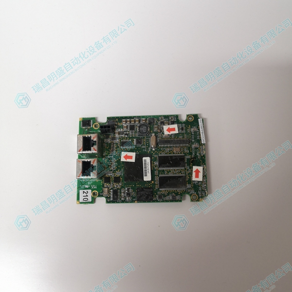
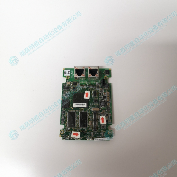
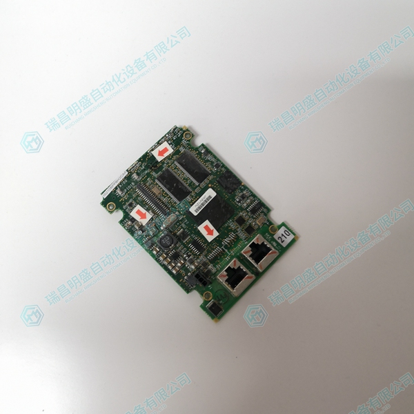
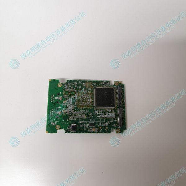
GE IS210BPPBH2CAA 印刷电路板
1.产 品 资 料 介 绍:
中文资料:
GE(通用电气)的印刷电路板(Printed Circuit Board,PCB)是一种用于支撑和衔接电子组件的症结元素。印刷电路板通常由导电资料制成,如铜,通过印刷、蚀刻等工艺造成电路板上的导电门路。它在电子装备和掌握体系中饰演着重要的脚色,供给了电气衔接和支撑电子元件的平台。
以下是一般性的印刷电路板的特征和功效:
电气衔接: PCB 供给了电子元件之间的电气衔接,通过导线和焊盘将各个元件衔接起来,造成一个完整的电路。
支撑元件: PCB 上通常有支架、孔位和其他构造,以支撑和装置电子元件,如电阻、电容、集成电路等。
导电层: PCB 上的导电层通常是用铜箔制成的,通过印刷或蚀刻工艺造成电路衔接。
条理构造: 多层 PCB 能够在不同的条理上安排导线和元件,以进步电路的复杂性和密度。
焊盘: 用于焊接元件的金属地区,保证电子元件与 PCB 之间的牢固衔接。
印刷标记: PCB 上通常印有标记、标记、编号等,以辅助辨认不同的元件和衔接。
英文资料:
GE's Printed Circuit Board (PCB) is a key element used to support and connect electronic components. Printed circuit boards are usually made of conductive materials, such as copper, which are used to create conductive circuits on the circuit board through processes such as printing and etching. It plays an important role in electronic equipment and control systems, providing a platform for electrical connection and supporting electronic components.
The following are the characteristics and functions of general printed circuit boards:
Electrical connection: PCB provides electrical connection between electronic components, connecting each component together through wires and pads, creating a complete circuit.
Supporting components: PCB usually has brackets, holes, and other structures to support and install electronic components such as resistors, capacitors, integrated circuits, etc.
Conductive layer: The conductive layer on a PCB is usually made of copper foil and is connected to the circuit through printing or etching processes.
Layered structure: Multilayer PCBs can arrange wires and components on different layers to improve the complexity and density of circuits.
Solder pad: A metal area used to weld components, ensuring a secure connection between electronic components and PCBs.
Printing marks: PCBs are usually printed with markings, markings, numbers, etc. to assist in identifying different components and connections.
2.产 品 展 示
")
3.主 营 品 牌
模块(图2)")
本篇文章出自瑞昌明盛自动化设备有限公司官网,转载请附上此链接:http://www.jiangxidcs.com