


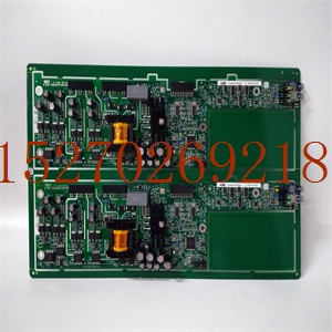
HIEE300024R4 UAA326A04机械设备卡件
并向出租车TX芯片提供传入字节的通知。3.串行差分信号驱动光纤驱动器通过光纤电缆向最多两个从模块发送数据。(主模块有两个信道,允许与两个从模块和两个接收器(如果选择)进行通信。从模块每个只有一个信道。)主模块和从模块之间的最大距离为1.4Km.a。如果没有来自发射机(HE697BEM713)的主模块(HE697FBX105)的输入信号:主模块通过AMD滑行发射机IC发送的定时同步脉冲继续保持与从模块的同步。b、 如果有来自发射机(HE697BEM713)的主模块(HE697FBX105)的输入信号:在持续500ns的转换过程中,主模块内发生延迟。延迟仅在有初始传入字节时发生。随后的比特不被延迟,因此,延迟不是累积的。3.1.3 HE697FBX100从模块1。从模块(HE697FBX100)通过光纤接收器接收输入的串行差分信号。(见图3.2)由于光纤电缆的传输时间,数据已延迟。延迟约为7ms。[通过玻璃]行驶1.4公里。第17页,1998年11月20日第3章:操作2。串行差分信号被路由到Taxi Rx1 IC,并被转换为8位并行格式。然后将8位并行格式发送到FPGA,在那里将其转换为数字逻辑。数字逻辑被发送到RS-422转换器,并被转换为RS-422信号。RS-422信号通过DB37退出从机,并发送至GE Fanuc Series 90-70 IC697BEM711接收器。a、 如果有来自HE697FBX105的输入信号进入HE697FBX100:由于从模块内的各种转换过程,存在1ms的延迟。3.接收机通过以上述过程的相反顺序将数据发送回从模块和主模块来响应来自发射机的请求。HE697BEM713发射器和IC697BEM711接收器通过光纤电缆(1.4公里)传输的数据的最大总延迟为17ms(往返延迟)。3.1.4电源1。提供的电源线用于从PLC提供+5 VDC电源。接口由2针可移动终端连接器和所提供电源电缆的DB9连接器组成。3.1.5故障检测1。除了用于状态和错误检测的LED指示灯外,还提供了外部故障电路,用于向远程位置发送输入,以帮助通知用户故障。外部故障指示器端口是一个3针可拆卸端子连接器,提供信号以允许故障检测。图3.1–主(HE697FBX105)图3.2–从(HE697FBX100)LED FPGA连接器DB37 RS-422转换器TAXI RX1 TAXI TX TAXI RX2 RX1 TX2 RX2 LED FPGA连接器DB27 RS-422转换器TAXI RX1 TAXI TX RX1 FO1 FO2 FAULT POWER POWER FAULT CH.3:操作1998年11月20日第18页3.2指示灯以下LED指示灯为HE697FBX100和HE697FBX105。表3.1和表3.2提供了指示器的说明。表3.1–主(HE697FBX105)指示灯的LED指示灯说明,表示电源“电源”指示灯。通电后,LED亮起。状态故障LED。FPGA编程后,此灯亮起。如果不是这样,或者如果TAXI芯片接收器检测到错误,它将关闭。信道1上的信道1 TX发射机活动。对于从属设备,仅存在通道1。信道1上的信道1 RX接收机活动。信道2上的信道2 TX发射机活动。信道2上的信道2 RX接收机活动。通道1的通道1开启状态。如果通道已激活,LED将亮起。通道2的通道2开启状态。如果通道已激活,LED将亮起。表3.2–LED说明
with the AMD Transmitter IC and provides notification to the Taxi TX chip of an incoming byte. 3. The serial differential signal drives the fiber optic drivers to send the data to up to two slave modules over a fiber optic cable. (The master has two channels allowing communication with two slave modules and two receivers, if selected. The slave modules only have one channel each.) The maximum distance between the master and slave modules is 1.4Km. a. If there is NO incoming signal to the master module (HE697FBX105) from the transmitter (HE697BEM713) : The master continues to maintain synchronization with the slave module(s) via a timing sync pulse sent by the AMD Taxi Transmitter IC. b. If there is an incoming signal to the master module (HE697FBX105) from the transmitter (HE697BEM713): A delay occurs within the master module during the conversion processes lasting 500ns. The delay only occurs when there is an initial incoming byte. Subsequent bits are not delayed, and thus, the delay is not cumulative. 3.1.3 HE697FBX100 Slave Module 1. The slave module (HE697FBX100) receives the incoming serial differential signal via the fiber optic receiver. (See Figure 3.2.) The data has been delayed due to travel time through the fiber optic cable. The delay is approximately 7ms. [through glass] for 1.4 Km. PAGE 17 20 NOV 1998 CH. 3: OPERATION 2. The serial differential signal is routed to the Taxi Rx1 IC and is converted into an 8-bit parallel format. The 8-bit parallel format is then sent to the FPGA where it is converted into digital logic. The digital logic is sent to the RS-422 Converter and is converted into RS-422 signals. The RS-422 signals exit the slave via the DB37 and are sent to the GE Fanuc Series 90-70 IC697BEM711 Receiver. a. If there is an incoming signal into the HE697FBX100 from HE697FBX105: Because of the various conversion processes within the slave module, there is a delay of 1ms. 3. The receiver responds to requests from the transmitter by sending data back to the slave and master modules in the reverse order of the processes described above. The total maximum delay of data from the HE697BEM713 Transmitter and the IC697BEM711 Receiver via fiber optic cable (1.4 Km.) is 17.ms (round trip delay). 3.1.4 Power 1. A supplied power cable is used to provide +5 VDC power from the PLC. . The interface consists of a 2-pin removable terminal connector and a DB9 Connector of the supplied power cable. 3.1.5 Fault Detection 1. In addition to LED indicators for status and error detection, an external fault circuit is also provided to send an input to a remote location to help notify the user of a fault. The external fault indicator port is a 3-pin removable terminal connector providing signals to allow fault detection. Figure 3.1 – Master (HE697FBX105) Figure 3.2 – Slave (HE697FBX100) LEDs FPGA Connector DB37 RS-422 Converter TAXI RX1 TAXI TX TAXI RX2 RX1 TX1 TX2 RX2 LEDs FPGA Connector DB37 RS-422 Converter TAXI RX1 TAXI TX RX1 TX1 FO1 FO2 FAULT POWER POWER FAULT CH. 3: OPERATION 20 NOV 1998 PAGE 18 3.2 Indicators The following LED indicators provide status and error detection for the HE697FBX100 and the HE697FBX105. Table 3.1 and Table 3.2 provide a description of the indicators. Table 3.1 – Description of LED Indicators for Master (HE697FBX105) Indicator Meaning POWER ‘Power’ indicator. Once power is applied, the LED lights. STATUS Fault LED. This lights once the FPGA is programmed. It turns off if this is not so or if a TAXI chip receiver has detected an error. Ch1 TX Transmitter activity on channel 1. For the slave, only channel 1 exists. Ch1 RX Receiver activity on Channel 1. Ch2 TX Transmitter activity on channel 2. Ch2 RX Receiver activity on channel 2. Ch1 ON Status of channel 1. If the channel is activated, the LED lights. Ch2 ON Status of channel 2. If the channel is activated, the LED lights. Table 3.2 – Description of LED
")
")
")
")

