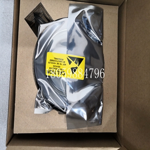
3BHL000397P0001 DCS模块
使用说明
定时器2 IRQ清除(T2IC)定时器2 IRQ-清除(T2IC)寄存器用于清除由定时器2引起的中断。写入该寄存器(位于BAR2地址偏移0x34处)将清除定时器2的中断。这也可以通过将“0”写入定时器控制状态寄存器(CSR1)的相应“定时器x引起的IRQ”字段来实现。此寄存器仅写,写入的数据不相关。定时器3 IRQ清除(T3IC)定时器3 IRQ-清除(T3IC)寄存器用于清除定时器3引起的中断。写入该寄存器(位于BAR2地址偏移0x38处)将清除定时器3的中断。这也可以通过将“0”写入定时器控制状态寄存器(CSR1)的相应“定时器x引起的IRQ”字段来实现。此寄存器仅写,写入的数据不相关。字段位读取或写入定时器4计数TMRCCR4[31..0]R.O.53定时器3定时器4 IRQ清除(T4IC)定时器4 IRQClear(T4C)寄存器用于清除定时器4引起的中断。写入此寄存器,位于距BAR2地址偏移0x3C处,可清除定时器4的中断。这也可以通过将“0”写入定时器控制状态寄存器(CSR1)的相应“定时器x引起的IRQ”字段来实现。此寄存器仅写,写入的数据不相关。54 3 VMIVME-7807/VME-7807RC产品手册看门狗定时器概述VMIVME-8807/VME-7807RC提供了一个可编程看门狗计时器(WDT),如果软件完整性出现故障,可用于重置系统。WDT控制状态寄存器(WCSR)WDT由位于BAR2地址偏移0x08处的WDT控制状况寄存器(WCSR)控制和监控。该寄存器中的位映射如下:“WDT Timeout Select”(WDT超时选择)字段用于选择看门狗定时器的超时值,如下所示:“SERR/RST Select”位用于选择WDT是在本地PCI总线上生成SERR#还是系统复位。如果该位设置为“0”,WDT将生成系统复位。否则,WDT将激活本地PCI总线SERR#信号。“WDT启用”位用于启用看门狗定时器功能。该位必须设置为“1”,以便看门狗定时器工作。请注意,由于所有寄存器在复位后默认为零,因此在复位后,看门狗定时器始终被禁用。
重新启用监视计时器
重置后,应用软件必须重新启用监视计时器,以便监视计时器继续运行。启用监视计时器后,应用程序软件必须在选定的超时时间内刷新监视计时器,以防止产生重置或SERR#。看门狗定时器为字段位读取或写入SERR/RST选择WCSR[16]R/W WDT超时选择WCSR[10..8]R/WWDT启用WCSR[0]R/W系统复位后,所有这些位默认为“0”。保留所有其他位。超时WCSR[10]WCSR[9]WCSR[8]135s 0 0 0 33.6s 0 0 1 2.1s 0 1 0 524ms 0 1 1 1 262ms 1 0 0 131ms 1 0 1 32.768ms 1 1 0 2.048ms 1 1 1 55通过写入WDT保活寄存器(WKPA)刷新看门狗计时器3。写入的数据无关。WDT保活寄存器(WKPA)启用时,通过在所选超时时间内写入位于BAR2地址偏移0x0C处的WDT保活寄存器(WKPIA),防止看门狗定时器重置系统。写入此位置的数据无关。56 3 VMIVME-7807/VME-7807RC产品手册NVRAM VMIVME-8807/VME-7807RC提供32KB的非易失性RAM。该内存映射到从BAR1地址开始的32K地址空间中。该内存随时可用,支持从PCI总线进行字节、短字和长字访问。当电路板的电源断开时,此存储器的内容将保留。57 VME控制3 VME控制下表显示了VMIVME-7807/VME-7807RC(从BAR0偏移)的寄存器定义。有关BAR0的更多信息,请参阅第47页的表3-1“PCI配置空间寄存器”。表3-2寄存器定义从BAR0寄存器名称偏移VMECOMM 0x00位名称位定义MEC_SEL 0主大端启用位1=大端,0=小端,SEC_SEL 1从大端启用比特1=大尾,0=小Endian ABLE 2辅助BERR逻辑使能位1=辅助。启用BERR 0=辅助。BERR禁用BTO 3总线错误计时器启用1=启用,0=禁用BTOV[1:0]5:4超时值00-16μs 01-64μs 10-256μs 11-1.00ms BERRI 6 BERR中断启用1=中断启用0=中断禁用BERRST 7 BERR状态读取/清除位1=清除BERR,0=不执行SFENA 8在WDT超时时启用VME SYSFAIL生成1=启用SYSFAIL,0=禁用未使用的9未使用的BPENA 10 Endian转换旁路位1=旁路,0=未旁路的VBENA 11 VME启用位(VBENA)1=启用,0=禁用的未使用的31:12未使用的VBAM 0x04 VME_ADDR 5:0锁存的VME地址修改器未使用的31
instructions
Timer 2 IRQ clear (T2IC) Timer 2 IRQ clear (T2IC) register is used to clear the interrupt caused by timer 2. Writing to this register (at BAR2 address offset 0x34) will clear the interrupt of timer 2. This can also be achieved by writing "0" to the corresponding "IRQ caused by timer x" field of the timer control status register (CSR1). This register is only for writing, and the written data is irrelevant. Timer 3 IRQ clear (T3IC) Timer 3 IRQ clear (T3IC) register is used to clear the interrupt caused by timer 3. Writing to this register (at BAR2 address offset 0x38) will clear the interrupt of timer 3. This can also be achieved by writing "0" to the corresponding "IRQ caused by timer x" field of the timer control status register (CSR1). This register is only for writing, and the written data is irrelevant. The field bit reads or writes the timer 4 count TMRCCR4 [31.0] R.O.53 timer 3 timer 4 IRQ clear (T4IC) timer 4 IRQClear (T4C) register to clear the interrupt caused by timer 4. Write this register at 0x3C offset from BAR2 address to clear the interrupt of timer 4. This can also be achieved by writing "0" to the corresponding "IRQ caused by timer x" field of the timer control status register (CSR1). This register is only for writing, and the written data is irrelevant. 54 3 VMIVME-7807/VME-7807RC Product Manual Overview of Watchdog Timer VMIVME-8807/VME-7807RC provides a programmable watchdog timer (WDT) that can be used to reset the system if software integrity fails. WDT control status register (WCSR) WDT is controlled and monitored by WDT control status register (WCSR) located at BAR2 address offset 0x08. The bit mapping in this register is as follows: "WDT Timeout Select" field is used to select the timeout value of the watchdog timer, as shown below: "SERR/RST Select" bit is used to select whether WDT generates SERR # on the local PCI bus or system reset. If this bit is set to "0", WDT will generate a system reset. Otherwise, WDT will activate the local PCI bus SERR # signal. The "WDT enable" bit is used to enable the watchdog timer function. This bit must be set to "1" for the watchdog timer to work. Note that since all registers default to zero after reset, the watchdog timer is always disabled after reset.
Re enable Watchdog Timer
After reset, the application must re enable the watchdog timer so that it can continue to run. When the watchdog timer is enabled, the application software must refresh the watchdog timer within the selected timeout to prevent a reset or SERR #. The watchdog timer selects WCSR [16] R/W WDT timeout for field bit reading or writing SERR/RST. Select WCSR [10.. 8] R/W WDT. After enabling WCSR [0] R/W system reset, all these bits are "0" by default. All other bits are reserved. Timeout WCSR [10] WCSR [9] WCSR [8] 135s 0 0 0 33.6s 0 1 2.1s 0 1 0 524ms 0 1 1 262ms 1 0 0 131ms 1 0 1 32.768ms 1 1 0 2.048ms 1 1 55 Refresh the watchdog timer 3 by writing the WDT active register (WKPA). The data written is irrelevant. When WDT keep alive register (WKPA) is enabled, the watchdog timer is prevented from resetting the system by writing the WDT keep alive register (WKPA) located at the BAR2 address offset 0x0C within the selected timeout. The data written to this location is irrelevant. 56 3 VMIVME-7807/VME-7807RC Product Manual NVRAM VMIVME-8807/VME-7807RC provides 32KB of non-volatile RAM. This memory is mapped to the 32K address space starting from the BAR1 address. This memory is readily available and supports byte, short word, and long word access from the PCI bus. When the power supply of the circuit board is disconnected, the contents of this memory will be retained. 57 VME control 3 VME control The following table shows the register definition of VMIVME-7807/VME-7807RC (offset from BAR0). For more information about BAR0, see Table 3-1 "PCI Configuration Space Registers" on page 47. Table 3-2 Register Definition Offset VMECOMM 0x00 Bit Name Bit Definition MEC from BAR0 Register Name_ SEL 0 main big end enable bit 1=big end, 0=small end, SEC_ SEL 1 enables bit 1=big tail from the big end, 0=small Endian ABLE 2 auxiliary BERR logic enable bit 1=auxiliary. Enable BERR 0=Auxiliary. BERR Disable BTO 3 Bus Error Timer Enable 1=Enable, 0=Disable BTOV [1:0] 5:4 Timeout value 00-16 μ s 01-64 μ s 10-256 μ S 11-1.00ms BERRI 6 BERR interrupt enable 1=interrupt enable 0=interrupt disable BERRST 7 BERR status read/clear bit 1=clear BERR, 0=do not execute SFENA 8 enable VME SYSFAIL generation when WDT timeout 1=enable SYSFAIL, 0=disable unused 9 unused BPENA 10 Endian conversion bypass bit 1=bypass, 0=VBENA 11 VME enable bit (VBENA) 1=enable, 0=disable unused 31:12 unused VBAM 0x04 VME_ ADDR 5:0 locked VME address modifier unused 31


