


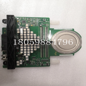
3BHB021400R0002工控模块PLC
eMMC引脚描述信号球号描述
时钟(CLK)M6时钟的每个周期在命令行和数据行上引导传输。命令(CMD)M信号是用于设备初始化和命令传输的双向命令通道。CMD信号有两种操作模式:开路漏极用于初始化,推挽式用于快速命令传输。数据(DAT0-DAT7)A3~AB2~B6这些是双向数据通道。DAT信号以推挽模式工作。RST_n K件复位输入DS H据选通:返回时钟信号,用于HS0模式VCCQ C6、MNP3、P源,用于MMC接口和控制器,有两种电源模式:高功率模式:2.7V~3.6V;低功耗模式:1.7V~1.9 VCC E6、FJ10、K9 NAND闪存电源,其电源电压范围为:2.7V~3.6V VDDi C2 VDDi为内部电源模式。将1uF或2.2uF电容器从VDDi连接到地VSS、VSSQ A6、E7、GH10、JJ8、CN2、PP6地线注意:所有其他引脚未连接[NC],可以连接到GND或左浮动。MKEV008GCB-SC0-8-DC电气特性1一般操作条件7参数符号最小最大单位备注所有线路上的峰值电压---0.VCCQ+0.V--所有输入输入泄漏电流(在初始化序列和/或连接内部上拉电阻器之前)---100 100 uA--输入泄漏电流(初始化序列和内部上拉电阻器断开后)---2 2 uA--所有输出输出漏电流(初始化序列前)---100 100 uA--输出漏电流。
工作电流
(RMS) 操作期间的有功功耗容量NAND型操作Icc Iccq单元(最大)(最大)8 GB 6b x 1读取70 200 mA写入 12mA注:-功率测量条件:总线配置=x8@200MHz DDR-最大RMS电流是100ms期间的平均RMS电流消耗。-温度:2-VCC=3.3V,VCCQ=1.8V-未100%测试MKEV008GCB-SC0-9-3电源电压参数符号测试条件最小最大单元电源电压1(NAND/核心)VCC-2.7 3.6 V电源电压2(CTRL/IO)VCCQ-1.7 1.9V 2.7 3.6 V机功耗 自动节能模式和待机状态下的待机功耗容量NAND类型状态Icc Iccq单元2828、8 GB 6b x 1待机20 100 600 uA注:-功率测量条件:总线配置=x8,无CLK-VCC=3.3V,VCCQ=1.8V-未100%测试眠功耗 休眠状态下的休眠功耗容量NAND类型状态Icc Iccq单元2828.8 GB 6b x 1休眠0.100 600 uA注:-功率测量条件:总线配置=x8,无CLK-通过CMD入休眠状态,VCC电源关闭,VCCQ=1.8V-未100%测试
EMMC pin description signal ball number description
Clock (CLK) Each cycle of M6 clock guides the transmission on the command line and data line. Command (CMD) M signal is a two-way command channel used for device initialization and command transmission. CMD signals have two operation modes: open drain for initialization and push-pull for fast command transmission. Data (DAT0-DAT7) A3~AB2~B6 These are two-way data channels. DAT signal operates in push-pull mode. RST_ N K piece reset input DS H is strobe: return clock signal is used for HS0 mode VCCQ C6, MNP3, P source, MMC interface and controller. There are two power modes: high power mode: 2.7V ~ 3.6V; Low power consumption mode: 1.7V ~ 1.9 VCC E6, FJ10, K9 NAND flash power supply, its power supply voltage range is 2.7V ~ 3.6V VDDi C2 VDDi is the internal power supply mode. Connect the 1uF or 2.2uF capacitor from VDDi to the ground wires of VSS, VSSQ A6, E7, GH10, JJ8, CN2 and PP6 Note: All other pins are not connected [NC], and can be connected to GND or left float. MKEV008GCB-SC0-8-DC Electrical characteristics 1 General operating conditions 7 Parameter symbols Minimum and maximum units Remarks Peak voltage on all lines -- -0.VCCQ+0. V -- All input and input leakage current (before initialization sequence and/or connection of internal pull-up resistor) -- 100 100 uA -- Input leakage current (after initialization sequence and internal pull-up resistor are disconnected) -- - 2 2 uA -- All output and output leakage current (before initialization sequence) ---100 100 uA - Output leakage current.
Operating current
(RMS) • Active power consumption capacity during operation NAND type operation Icc Iccq unit (maximum) (maximum) 8 GB 6b x 1 Read 70 200 mA Write 12 mA Note: - Power measurement conditions: bus configuration= x8@200MHz DDR - The maximum RMS current is the average RMS current consumption during 100ms- Temperature: 2-VCC=3.3V, VCCQ=1.8V - not 100% tested MKEV008GCB-SC0-9-3 power supply voltage parameter symbols Test conditions Minimum maximum unit power supply voltage 1 (NAND/core) VCC-2.7 3.6 V power supply voltage 2 (CTRL/IO) VCCQ-1.7 1.9V 2.7 3.6 V unit power consumption Standby power consumption capacity in automatic energy-saving mode and standby mode NAND type status Icc Iccq unit 2828, 8 GB 6b x 1 Standby 20 100 600 uA Note: - Power measurement conditions: bus configuration=x8, No CLK-VCC=3.3V, VCCQ=1.8V - No 100% test of sleep power consumption • Sleep power consumption capacity in sleep state NAND type state Icc Iccq unit 2828.8 GB 6b x 1 sleep 0.100 600 uA Note: - Power measurement conditions: bus configuration=x8, no CLK - No sleep state through CMD, VCC power off, VCCQ=1.8V - No 100% test
")
")
")

