


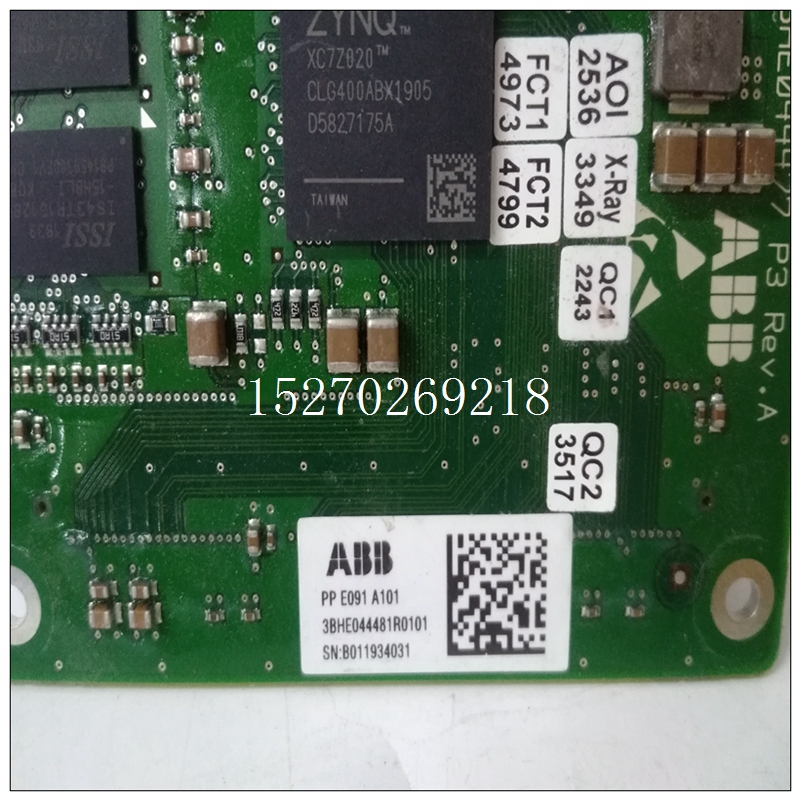
PPE091A101使用尺寸,ABB控制模块
如第3.2节所述,Pl/T模块的操作可能受到以下限制:八进制缓冲器用于将端口数据驱动到P3和P4连接器。此限制限制某些端口模式的使用,例如双向数据传输。之前阅读下一节,读者应该了解程序员本手册附录中MC68230数据规范的型号部分。用户还需要阅读第5.2节,以确保编程一致在为VMIVME-2511供电之前,使用110个端口的跳线配置。对于关于中断的编程,读者应该了解附录中引用的BIM,用于补充BIM编程描述如下。
")
PPE091A101使用尺寸4.2 BIM和PIIT寄存器映射MC68153 BIM包含八个8位寄存器,而PI/T模块分别包含八个8位寄存器包含32个8位寄存器,其中仅使用25个。所有寄存器均位于奇数字节位置。BIM寄存器映射如表4-1所示。VMIVME-2511在工厂配置为响应短路监控110访问,但可以配置为通过以下方式响应短期非特权输入/输出访问:安装跳线,见第5.1节。在15个地址位A1-A15中,只有8个(A15-A8)被解码以进行电路板选择。地址选择见第5.3节开关。Pl/T#1寄存器映射如表4-2所示(4页)。PIIT#2寄存器映射如表4-3(4页)所示。MC68153 BIM上的八个8位寄存器作为奇数字节访问位置。每个寄存器的位定义可在MC68153 BIM中找到附录中的规范。
每个MC68230 Pl/T模块上的32个8位寄存器访问如下:奇数字节位置。每个寄存器的位定义可以在MC68230中找到PIIT规范见附录。编程MC68153 BIM由于Plfr模块提供它们自己的中断向量。因此,必须针对外部矢量对BIM进行编程。此外,每个中断源对应的中断自动清除位必须为set(高电平)及其相关的中断启用位。这将需要每次中断时用于设置中断启用位的中断服务例程已处理。中断向量由中断PIIT模块在中断期间提供确认周期。这些矢量由端口中断矢量寄存器提供并通过PIE模块上的定时器中断矢量寄存器,具体取决于正在确认哪个中断源。
BIM板上的控制寄存器与PllT中断相关通道如下所示。
As stated in Section 3.2, the operation of the Pl/T module can be limited due to
octal buffers being used to drive port data to the P3 and P4 connectors. This limitation
restricts the use of some port modes, such as bi-directional data transfer. Before
reading the next section the reader should have an understanding of the Programmers
Model section of the MC68230 data specifications in the appendices of this manual.
The user will also want to read Section 5.2 such that the programming is consistent
with the jumper configuration of the 110 ports before powering the VMIVME-2511. For
programming concerning interrupts, the reader should have an understanding of the
BIM which is referenced in the appendices to supplement the BIM programming
description which follows.
4.2 BIM AND PIIT REGISTER MAP
The MC68153 BIM contains eight 8-bit registers while the PI/T modules each
contain 32 eight-bit registers of which only 25 are used. All registers are addressed on
odd-byte locations. The BIM register map is shown in Table 4-1.
The VMIVME-2511 is factory configured to respond to Short Supervisory 110
Access, but can be configured to respond to Short Non-Privileged I/O Access by
installing a jumper, see Section 5.1. Of the 15 address bits A1-A15, only eight
(A15-A8) are decoded for board select. See Section 5.3 for address selection
switches. The Pl/T #1 register map is shown in Table 4-2 (4 pages). The PIIT #2
register map is shown in Table 4-3 (4 pages).
The eight 8-bit registers on board the MC68153 BIM are accessed as odd byte
locations. The bit definition of each register can be found in the MC68153 BIM
specifications in the appendices.
The 32 eight-bit registers on board each MC68230 Pl/T modules are accessed as
odd-byte locations. The bit definition of each register can be found in the MC68230
PIIT specifications in the appendices. PROGRAMMING THE MC68153 BIM
The vector registers on-board the BIM are not used since the Plfr modules supply
their own interrupt vector. Therefore, the BIM must be programmed for external vectors.
In addition, the interrupt auto-clear bit corresponding to each interrupt source must be
set (high level), along with its associated interrupt enable bit. This will require the
interrupt service routine to be used to set the interrupt enable bit each time an interrupt
is processed. The interrupt vector is supplied by the interrupting PIIT module during an interrupt
acknowledge cycle. These vectors are supplied by the Port lnterrupt Vector Register
and by the Timer lnterrupt Vector Register on board the PIE module, depending on
which interrupt source is being acknowledged.
The control registers on-board the BIM are associated with the PllT interrupt
channels as shown below.

