


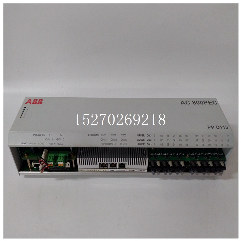
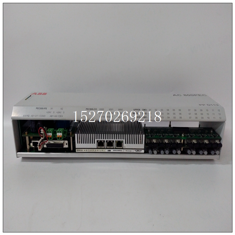
PPD113B01-10-150000控制器,ABB处理卡件
并行I10端口可编程为允许单向8位端口,双向8位端口和位I10(8位端口中的每个位方向都是可编程的。高电流驱动器选项可用。当采用大电流选项时8位端口仅可编程用于单向输出或输入。
2.2功能特性:兼容性:VMEbus规格兼容双高形状系数I10连接器类型:64针连接器DIN 41 61 2110组织:251 1板使用两个摩托罗拉MC68230并行接口定时器,提供多种可编程I10功能,包括位110,单向$-位和16位输入/输出,双向8位和16位110,可选握手选项和24位可编程定时器。
")
PPD113B01-10-150000控制器251 1可能是订购时带有缓冲110选项,可提供多达64mA接收器能力;然而,双向此选项不支持模式。此外如果选择位I10模式,则所有端口A数据位必须按相同方向编程。一个八位DIP开关提供电路板住址251 1在工厂配置为响应短监督输入/输出访问;
但是,用户可以将跳线更改为启用短非特权I10访问。方块图VMIVME-2511由10个主要子系统组成,如图3-1所示。每个子系统进一步分解为详细的框图,如所示图3-2至3-4。3.2操作概述如图3-1中的功能框图所示,VMIVME-2511利用两个MC68230模块。每个MC68230并行接口定时器模块(PI/T)有3个110个端口和一些额外的握手接口。握手信号和输入/输出每个模块的端口依次映射到单个110连接器。模块将在讨论中提及与P3连接器相关的如下所示。与P4连接器相关的模块将为称为Pl/T#2。要使用VMIVME-2511执行110次数据传输,请在两个Pl/T模块的选择取决于输入或输出数据传输连接P3或P4。为了使用VMIVME-2511实现中断处理,选择了PIIT模块为端口或定时器中断编程。然后是68153总线中的正确通道启用中断器模块(BIM),允许特定的中断源由系统处理器确认。由于以下原因,需要选择一些跳线:Plrr模块的端口通道可以用作110通道或中断当缓冲器选项信号方向也为跳投。
The parallel I10 ports are programmable to allow unidirectional 8-bit ports,
bidirectional 8-bit ports and bit I10 (each bits direction in a 8-bit port is programmable.
A high current driver option is available. When the high current option is employed, the
8-bit ports are programmable for unidirectional only, either outputs or inputs.
2.2 FUNCTIONAL CHARACTERISTICS:
Compatibility: VMEbus Specification Compatible Double-Height
Form Factor
I10 Connector Type: 64-pin connector-DIN 41 61 2
110 Organization: The 251 1 board utilizes two Motorola MC68230
Parallel Interfacerrimers that provide a wide variety of
programmable I10 features including bit 110,
unidirectional $-bit and 16-bit I/O, bi-directional 8-bit
and 16-bit 110, selectable handshaking options and
a 24-bit programmable timer. The 251 1 may be
ordered with a buffered 110 option that provides up to
64mA sink capability; however, the bi-directional
modes are not supported with this option. In addition,
if the bit I10 mode is chosen, all Port A data bits must
be programmed in the same direction. One eight position DIP switch provides the board
address. The 251 1 is configured at the factory to
respond to short supervisory I/O access;
however, the user may change the jumper to enable
short non-privileged I10 access. BLOCK DIAGRAMS
The VMIVME-2511 consists of 10 major subsystems as illustrated in Figure 3-1.
Each subsystem is further broken down into detailed block diagrams as shown in
Figures 3-2 through 3-4.
3.2 OPERATIONAL OVERVIEW
As noted in the functional block diagram in Figure 3-1, the VMIVME-2511 utilizes
two MC68230 modules. Each MC68230 Parallel InterfaceiTimer module (PI/T) has 3
110 ports and some additional handshake interface. The handshake signals and the I/O
ports of each module are in turn mapped into a single 110 connector. The module
which is associated with the P3 connector will be referred to in the discussion which
follows as Pl/T #I. The module which is associated with the P4 connector will be
referred to as Pl/T #2.
To perform 110 data transfers with the VMIVME-2511, registers on board the two
Pl/T modules are selected for either input or output data transfers depending on which
connector, P3 or P4, is to be accessed. To achieve interrupt processing with the VMIVME-2511, the chosen PIIT module
is programmed for port or timer interrupts. Then the proper channel in the 68153 Bus
Interrupter Module (BIM) is enabled allowing the particular interrupt source of interest to
be acknowledged by the system processor. Some jumper selection is required due to
the port channels of the Plrr modules which can serve as 110 channels or interrupt
request or acknowledge signals when the buffer option signal direction is also
jumpered.

