


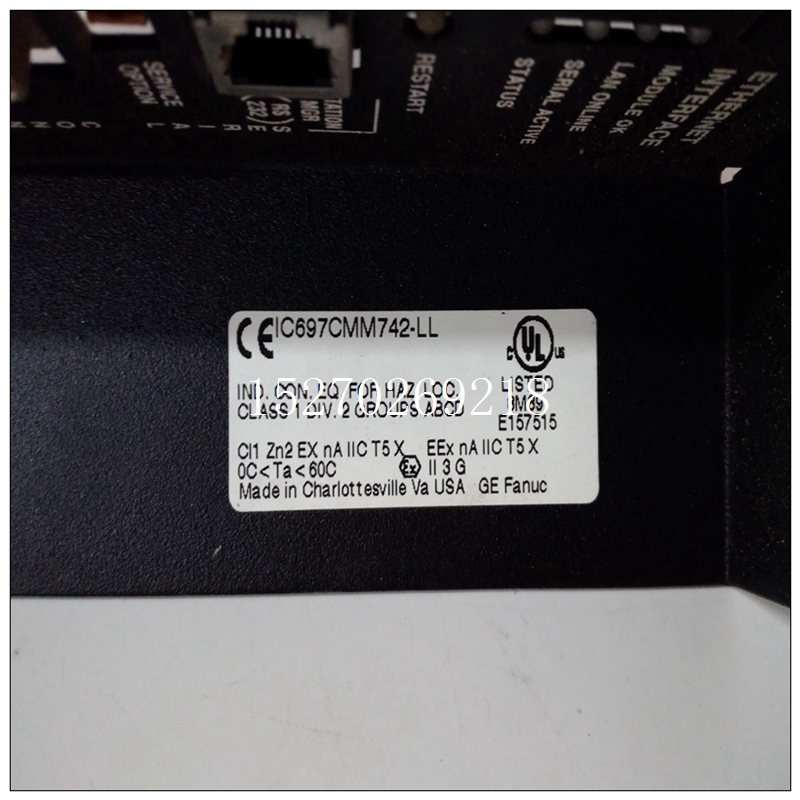
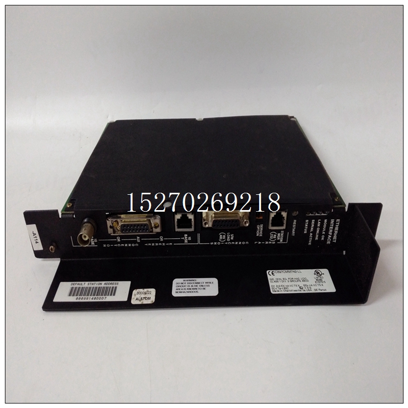
IC697CMM742-LL使用指导,GE通用电气
可编程增益跳线配置增益放大器可配置为1、10、100、200和500以处理低至±10 mV的信号电平。表5.4.7-1显示了哪个跳线将安装。该电路板在工厂配置为增益“一”(无跳线)已安装)。5.5校准出厂前,VMIVME-3112板已完全校准并符合第2节中列出的所有规范。应该然而,需要重新校准,执行第5.5.2节和5.5.3使用第5.5.1节中列出的设备。所有调整的位置和测试点如图5.4-1所示。出厂时,所有校准调整均密封防止意外移动。密封件很容易被打破以进行重新校准,然而所有调整均应使用合适的密封件重新密封完成重新校准后的化合物。
")
IC697CMM742-LL使用指导所需设备
a、 数字电压表(DVM)。±1.0000 VDC和±10.000 VDC范围;5.或更多数字;读数电压测量值的±0.005%精确10米Ω 最小输入阻抗。b、 模拟电压源。±10.000 VDC范围;分辨率0.0005
VDC;精度,预期值的±0.005%;0.10Ω 最大限度输出阻抗。c、 底盘。VMEbus背板或等效物,J1和J2连接器,VMEbus主控制器,+5±0.1 VDC,电源。一个插槽分配用于测试VMIVME-3112板。d、 延长板。VMEbus扩展板。e、 测试电缆。测试上述设备的电缆。5.5.2模拟输入校准程序校准包括将转换器的最大负输出调整为其理想值(偏移调整),然后将最大正输出调整为其理想值值(增益调整)。在更换时必须执行校准A/D的输入满标度范围从一个值到另一个值(例如,从±10 V到±5 V)。程序如下:a、 将VMIVME-3112板安装在VMEbus的扩展板上背板。b、 将模拟输入配置为所需的电压范围(即±10 V,±5 V,0至+10 V)。c、 给背板通电。允许最小预热间隔为通电后10分钟后继续。d、 将模拟电压源连接在连接器引脚之间的CH0处P3-A1(+)和P3-C1(-)。e、 调整模拟电压源以进行最负校准所选满标度范围的值。见表5.5.2-1。f、 读取CH0时,调整R4的单极范围或R8的双极范围角。CH0地址为XXXX0080。继续调整电位计,直到读取的值在000 HEX和001之间闪烁十六进制。
g、 调整模拟电压源以进行最正向校准所选满标度范围的值。见表5.5.2-1。h、 读取CH0时,调整R9,直到读取的值在FFE和FFF六角。i、 校准现已完成。拆除所有测试连接,以及将电路板恢复到其原始配置。
Programmable Gain Jumper Configuration
The Gain Amplifier may be configured for gains of 1, 10, 100, 200, and
500 to handle signal levels as low as ±10 mV. Table 5.4.7-1 shows which jumper
is to be installed. The board is factory configured for a gain of "one" (no jumper
installed).
5.5 CALIBRATION
Before delivery from the factory, the VMIVME-3112 Board is fully
calibrated and conforms to all specifications listed in Section 2. Should
recalibration be required, however, perform the procedures in Sections 5.5.2 and
5.5.3 with the equipment listed in Section 5.5.1. The locations of all adjustments and
test points are shown in Figure 5.4-1.
As delivered from the factory, all calibration adjustments are sealed
against accidental movement. The seals are easily broken for recalibration,
however. All adjustments should be resealed with a suitable fact curing sealing
compound after recalibration has been completed. Equipment Required
a. Digital Voltmeter (DVM). ±1.0000 VDC and ±10.000 VDC ranges; 5
or more digits; ±0.005 percent of reading voltage measurement
accuracy; 10 MΩ minimum input impedance.
b. Analog Voltage Source. ±10.000 VDC Range; resolution 0.0005
VDC; Accuracy, ±0.005 percent of expected value; 0.10 Ω maximum
output impedance.
c. Chassis. VMEbus backplane or equivalent, J1 and J2 connectors,
VMEbus master controller, +5 ±0.1 VDC, power supply. One slot
allocated for testing the VMIVME-3112 Board.
d. Extender Board. VMEbus extender board.
e. Test Cables. Test cables for the equipment listed above.
5.5.2 Analog Inputs Calibration Procedure
Calibration consists of adjusting the converter's most negative output to
its ideal value (offset adjustment), next adjusting the most positive output to its ideal
value (Gain Adjustment). The calibration must be performed when changing the
A/D's input full scale range from one value to another (for example, from ±10 V to
±5 V). The procedure is as follows:
a. Install the VMIVME-3112 Board on an extender board in a VMEbus
backplane.
b. Configure the analog inputs to the desired voltage range (i.e. ±10 V,
±5 V, 0 to +10 V). c. Apply power to the backplane. Allow a minimum warm up interval of
ten minutes after power has been applied before proceeding.
d. Connect the analog voltage source at CH0, between connector pins
P3-A1 (+) and P3-C1 (-).
e. Adjust the analog voltage source for the most negative calibration
value of the full scale range selected. Refer to Table 5.5.2-1.
f. While reading CH0 adjust R4 for unipolar ranges or R8 for bipolar
angles. CH0 address is XXXX0080. Continue adjusting the
potentiometer until the value read flickers between 000 HEX and 001
HEX.
g. Adjust the analog voltage source for the most positive calibration
value of the full scale range selected. Refer to Table 5.5.2-1.
h. While reading CH0 adjust R9 until the value read flickers between
FFE and FFF HEX.
i. Calibration is now complete. Remove all test connections, and
restore the board to its original configuration.

