


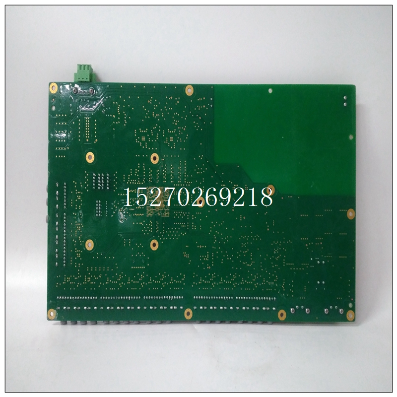
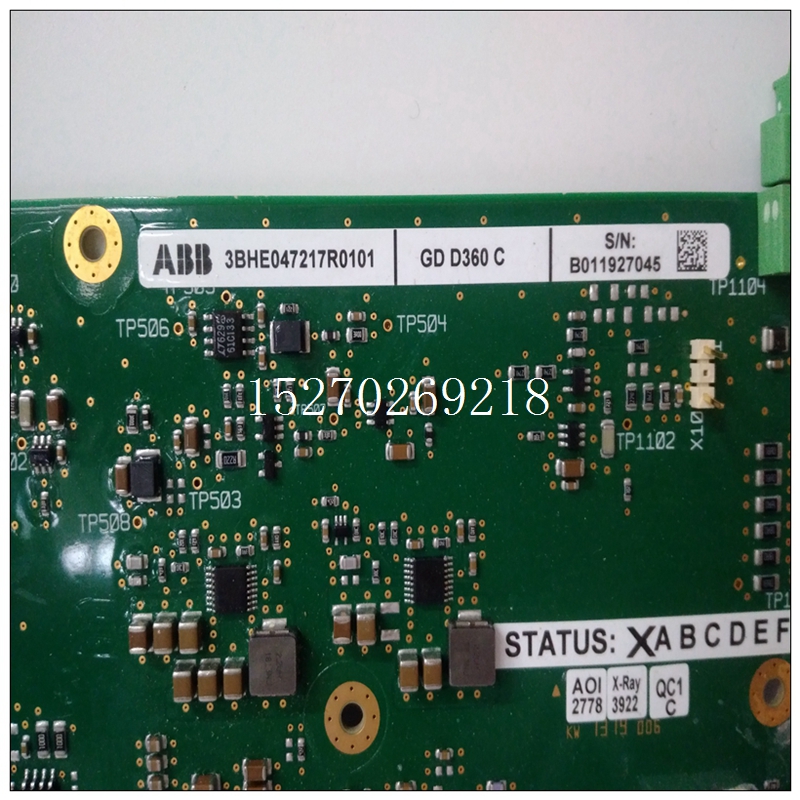
GDD360C用户手册,ABB工控卡件
电路板ID寄存器VMIVME-3112寄存器集的第一个字位置是只读寄存器。它总是读取08XX(十六进制;最后两位数字不是指定)。其他VMIC产品具有类似的寄存器,其读取的数据不同常数。这允许通用系统软件自动确定安装了哪些板(通过读取预定的地址列表)。配置软件必须能够处理总线如果它可能读取空位置,则出错。
")
GDD360C用户手册3.12内置功率转换器VMIVME-3112模拟网络的电源由直流-直流转换器如图3.12-1所示。转换器转换5 V逻辑电源转换为稳压和隔离的±15 VDC电源,负载容量为每个15 V总线上约100 mA。引言通过128与VMIVME-3112通信映射到VME短输入/输出的连续16位寄存器位置地址空间。大多数VMEbus CPU访问较短的I/O空间,就好像它是一个传统内存的64 KB块。请参阅CPU手册以确定此块的地址。
VMIVME-3112支持字节和字(16位)访问。订单一个字中的字节数取决于所用CPU的型号。例如,大多数基于68000的CPU将最高有效字节放在与字相同的地址。最低有效字节位于下一个地址。注意,如果AUTOSCAN数据为读作两个字节,它们可能来自不同的转换周期。这个可以在读数中引入256计数错误。详细讨论了通信寄存器的功能在本节中,总结见表4.1-1。有些寄存器不是已使用,并标记为“保留”。保留寄存器可能是重复映射正常控制寄存器。不应使用它们,因为它们可能会受到影响通过设计变更。4.2控制和状态寄存器说明位于相对地址02H的通信寄存器是控制和状态寄存器(CSR),并包含控制和监控以下电路板操作:a、 模拟输入通道选择b、 A/D操作模式c、 开始A/D转换d、 启动可编程定时器e、 二的补码选择f、 前面板故障指示灯g、 电路板重置h、 增益延迟
BOARD ID REGISTER
The first word location of the VMIVME-3112's register set is a
read-only register. It always reads 08XX (HEX; the last two digits are not
specified). Other VMIC products have similar registers which read different
constants. This allows general-purpose system software to automatically
determine what boards have been installed (by reading from a predetermined
list of addresses). The configuration software must be able to handle a bus
error if it might read an empty location.
3.12 BUILT-IN POWER CONVERTER
Electrical power for the VMIVME-3112 analog network is supplied by
the DC-to-DC converter shown in Figure 3.12-1. The converter transforms 5 V
logic power into regulated and isolated ±15 VDC power, with a load capacity of
approximately 100 mA on each 15 V bus. INTRODUCTION
Communication with the VMIVME-3112 takes place through 128
contiguous, 16-bit register locations which are mapped into the VME short I/O
address space. Most VMEbus CPUs access the short I/O space as if it were a
64-Kbyte block of conventional memory. Consult your CPU manual to determine
the address of this block.
The VMIVME-3112 supports byte and word (16-bit) accesses. The order
of the bytes within a word depends on the model of CPU used. For instance, most
68000-based CPUs put the most significant byte at the same address as the word.
The least significant byte is at the next address. Note that if the AUTOSCAN data is
read as two bytes, they may be from different conversion cycles. This can
introduce a 256-count error in the reading.
Functions of the communications registers, which are discussed in detail
within this section, are summarized in Table 4.1-1. Some of the registers are not
used, and are labeled "reserved". Reserved registers may be duplicate mappings
of normal Control Registers. They should not be used, since they could be affected
by a design change.
4.2 CONTROL AND STATUS REGISTER DESCRIPTIONS
The communication register located at relative address 02H is the
Control and Status Register (CSR), and contains all of the flags necessary to
control and monitor the following board operations:
a. Analog input channel selection
b. A/D operating modes
c. Start A/D conversion
d. Start Programmable Timer
e. Two's complement selection
f. Front panel Fail Indicator
g. Board RESET
h. Gain Delay

