


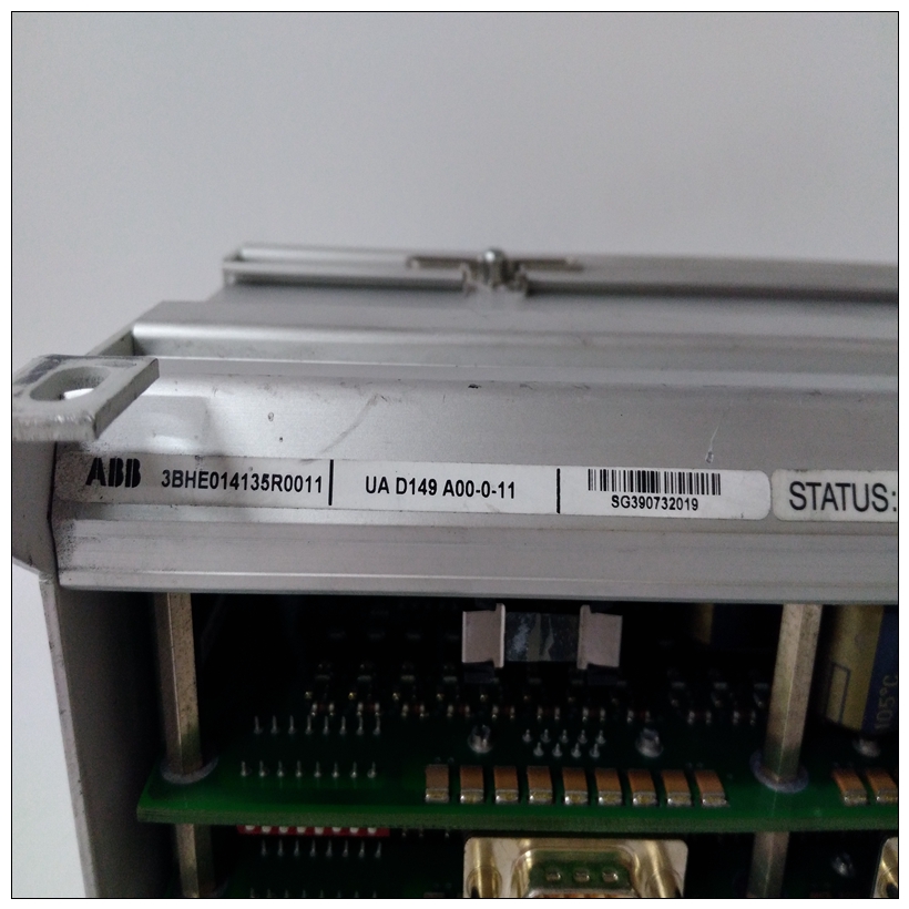
UAD149自动化模块,ABB使用方法
缓存模式控制(J3)MVME2603/2604上有256KB的二级缓存。L2缓存操作对用户是透明的,但其直写模式是可通过旧板上的头J3配置。在更新的MVME2603/2604上未提供板头J3。J3上安装跳线后,缓存直写在CPU控制下。拆下跳线后,缓存在所有情况下都会发生直写。闪存组选择(J10)MVME2603/2604基板提供1MB 16位闪存记忆力RAM200内存夹层可容纳4MB或8MB额外的64位闪存。
")
UAD149自动化模块闪存被组织在一个或两个组中,每个组16位或64位宽。两个银行都有车载调试器,PPCBug。要启用闪存组A(驻留在RAM200夹层上的焊接设备上的4MB或8MB固件),请在标头J10上放置一根跳线针脚1和2。启用闪存组B(位于插槽中的1MB固件在基板上),在收割台J10针脚2和3之间放置跨接导线。串行端口4接收时钟配置(J16)在同步串行通信中,您可以在上配置串行端口4MVME2603/2604使用RxC信号提供的时钟信号线在MVME712M兼容版本的基板上,标题J16将端口4配置为驱动或接收RxC。工厂配置将端口4设置为接收RxC。J16在MVME761兼容上保持打开状态版本。要完成串行端口4的配置,必须设置以下内容
配置标头:❏ J17(串行端口4传输时钟配置)❏ J20(串口4发送时钟接收器缓冲控制)
❏ MVME712M过渡模块上的J15或MVME761上的J3转换模块(串行端口4时钟配置)
图1-9和图1-10(适用于MVME712M)以及图1-14和图1-15(对于MVME761)显示了整体跳线设置串行端口的MVME2603/2604和转换模块上需4 DCE或DTE配置。
有关这些标头配置的更多详细信息,请参阅MVME712M过渡模块准备,第1-14页,MVME761第1-25页的过渡模块准备,或各用户的过渡模块手册(见附录D,相关文件)。
Cache Mode Control (J3)
256KB of L2 cache memory is available on the MVME2603/2604. L2
cache operation is transparent to users, but its write-through mode is
configurable via header J3 on older boards. On newer MVME2603/2604
boards, header J3 is not provided. With a jumper installed on J3, cache
write-through is under CPU control. With the jumper removed, cache
write-through occurs in all cases.Flash Bank Selection (J10)
The MVME2603/2604 base board has provision for 1MB of 16-bit Flash
memory. The RAM200 memory mezzanine accommodates 4MB or 8MB
of additional 64-bit Flash memory.
The Flash memory is organized in either one or two banks, each bank
either 16- or 64-bits wide. Both banks contain the onboard debugger,
PPCBug.
To enable Flash bank A (4MB or 8MB of firmware resident on solderedin devices on the RAM200 mezzanine), place a jumper across header J10
pins 1 and 2. To enable Flash bank B (1MB of firmware located in sockets
on the base board), place a jumper across header J10 pins 2 and 3.Serial Port 4 Receive Clock Configuration (J16)
In synchronous serial communications, you can configure Serial Port 4 on
the MVME2603/2604 to use the clock signals provided by the RxC signal
line. On MVME712M-compatible versions of the base board, header J16
configures port 4 to either drive or receive RxC. The factory configuration
has port 4 set to receive RxC. J16 remains open on MVME761-compatible
versions.
To complete the configuration of Serial Port 4, you must set the following
configuration headers as well:
❏ J17 (Serial Port 4 transmit clock configuration)
❏ J20 (Serial Port 4 transmit clock receiver buffer control)
❏ J15 on the MVME712M transition module or J3 on the MVME761
transition module (Serial Port 4 clock configuration)
Figure 1-9 and Figure 1-10 (for the MVME712M) and Figure 1-14 and
Figure 1-15 (for the MVME761) diagram the overall jumper settings
required on the MVME2603/2604 and transition module for a Serial Port
4 DCE or DTE configuration.
For additional details on the configuration of those headers, refer to
MVME712M Transition Module Preparation on page 1-14, MVME761
Transition Module Preparation on page 1-25, or to the respective user’s
manuals for the transition modules (listed in Appendix D, Related
Documentation) as necessary.

