


Brooks Automation 002-7391-25晶圆对准器 PDF资料
1.产 品 资 料 介 绍:
中文资料:
Brooks Automation 002-7391-25 晶圆对准器是一种高精度的设备,主要用于半导体制造和材料科学领域,确保晶圆在加工过程中的精确对位。该对准器能够显著提高晶圆加工的效率和质量,特别是在需要高精度对准的应用中。
主要特点:
高精度对准:
- 具备高精度的光学和机械对准系统,确保晶圆在处理过程中的准确定位,降低位置误差。
快速响应:
- 设计优化,提供快速的对准速度,能够在短时间内完成对准过程,提高生产效率。
用户友好界面:
- 提供直观的操作界面,使用户可以方便地设置和调整对准参数,简化了操作流程。
耐用材料:
- 采用高耐磨和耐腐蚀的材料,确保设备在严苛的工业环境中长期稳定运行。
兼容性强:
- 可与多种自动化设备和控制系统兼容,方便集成到现有生产线中。
实时监控:
- 具备实时监控和数据记录功能,用户可以随时查看对准状态和历史数据,有助于质量控制。
应用领域:
半导体制造:
- 在晶圆加工过程中,确保晶圆的精确对位,是提升良率和产品质量的关键环节。
材料科学研究:
- 用于材料科学实验中的样品对准,帮助科学家进行高精度实验。
光刻工艺:
- 在光刻过程中,对晶圆进行准确对准,以确保图形的精确转移。
电子组件组装:
- 在电子产品组装过程中,进行元件和基板的对准,以提高组装的精度和效率。
英文资料:
The Brooks Automation 002-7391-25 wafer aligner is a high-precision device primarily used in semiconductor manufacturing and materials science to ensure precise alignment of wafers during processing. This aligner can significantly improve the efficiency and quality of wafer processing, especially in applications that require high-precision alignment.
Main features:
High precision alignment:
Equipped with high-precision optical and mechanical alignment systems, ensuring accurate positioning of wafers during processing and reducing positional errors.
Quick response:
Design optimization, providing fast alignment speed, can complete the alignment process in a short time, and improve production efficiency.
User friendly interface:
Providing an intuitive user interface allows users to easily set and adjust alignment parameters, simplifying the operation process.
Durable materials:
Using highly wear-resistant and corrosion-resistant materials to ensure long-term stable operation of the equipment in harsh industrial environments.
Strong compatibility:
Compatible with various automation equipment and control systems, making it easy to integrate into existing production lines.
Real time monitoring:
Equipped with real-time monitoring and data recording functions, users can view alignment status and historical data at any time, which helps with quality control.
Application areas:
Semiconductor manufacturing:
Ensuring precise alignment of wafers during wafer processing is a key step in improving yield and product quality.
Materials Science Research:
Used for sample alignment in materials science experiments, helping scientists conduct high-precision experiments.
Lithography process:
During the photolithography process, the wafer is accurately aligned to ensure precise transfer of patterns.
Electronic component assembly:
During the assembly process of electronic products, alignment of components and substrates is carried out to improve the accuracy and efficiency of assembly.
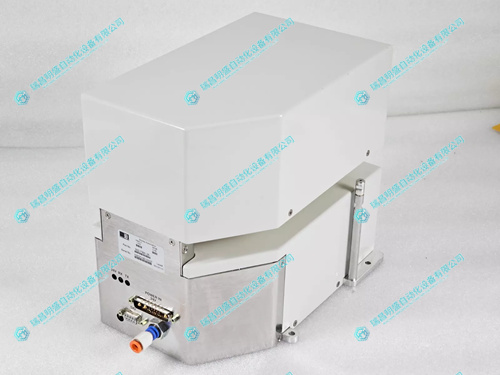
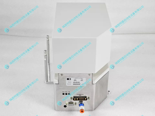
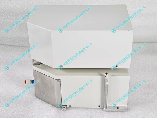
2.产 品 展 示
")
3.其他产品
BENTLY 3500/22M 146031-01瞬态数据接口模块
4.其他英文产品
ASEA 57360001-AN circuit board
ASEA DSQC108 controller backplane
5.更多库存型号
| PMB31D-10114-03 | NKMP11 | M22NRXB-LNN-NS-02 |
| PMB31D-10114-02 | AMAT 0100-13011 | 57160001-LF DSTD 133 |
| PMB31D-10114-01 | 70 FA 01b | PWM3636-5486-7 |
| PMB31D-10114-00 | IIMCL01 | 57160001-FH DSTD 170 |
| PMB31D-10101-03 | 70 BL 02C | N42HRFM-LNK-NS-00 |
| PMB31D-10101-02 | AMAT 0100-09136 | 57120001-HP DSTA 145 |
| PMB31D-10101-01 | 07YS81 | P21NSXC-LNN-NS-04 |
本篇文章出自瑞昌明盛自动化设备有限公司官网,转载请附上此链接:http://www.jiangxidcs.co

