


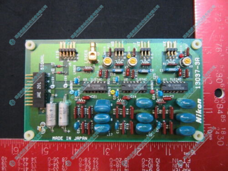
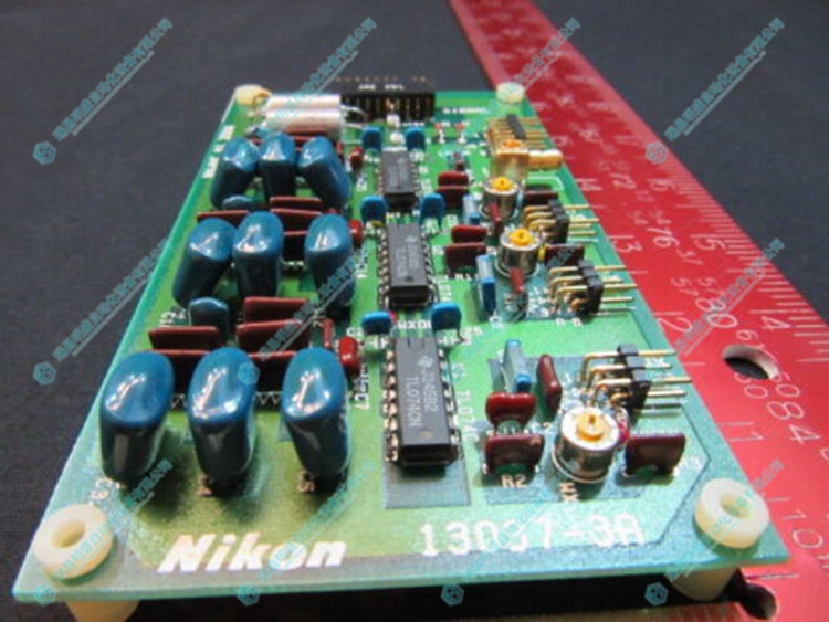
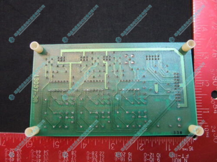
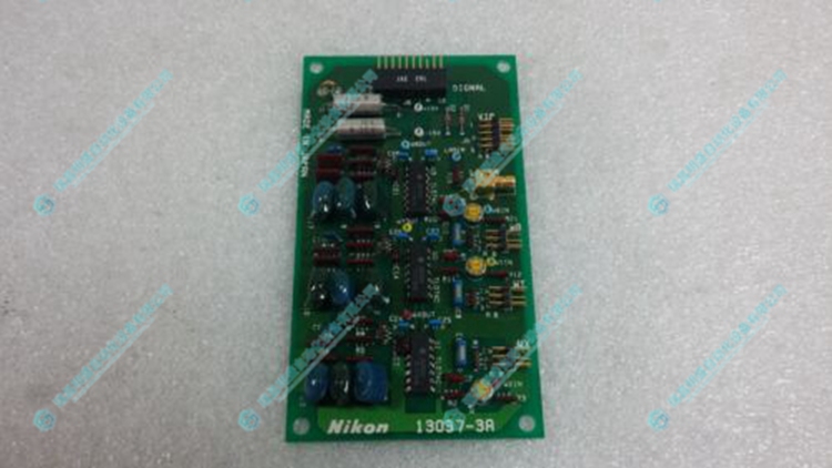
Nikon 13037-3A 晶圆对准器
1.产 品 资 料 介 绍:
中文资料:
ikon 13037-3A晶圆对准器主要用于光学系统和显微镜系统,例如用于显微观察、测量、分析和检验等领域。
具体来说,Nikon 13037-3A晶圆对准器可以应用于以下领域:
- 半导体制造:在半导体制造过程中,晶圆对准器被用于将晶圆进行精确对准,以确保半导体器件的制造精度和性能。
- 光学测量:Nikon 13037-3A晶圆对准器可以作为光学系统的一部分,用于进行各种光学测量和检验,例如显微观察、表面形貌测量、光学分析等。
- 生物医学研究:在生物医学领域,Nikon 13037-3A晶圆对准器可以用于制作样本、观察细胞结构、分析生物样品等。
- 微电子学:在微电子学领域,晶圆对准器被用于在微米甚至纳米级别进行精确对准和测量,以确保微电子器件的制造精度和质量。
- 材料科学:在材料科学领域,Nikon 13037-3A晶圆对准器可以用于观察和分析材料显微结构、表面形貌等,以帮助研究人员了解材料的性质和性能。
总之,Nikon 13037-3A晶圆对准器在光学、半导体、生物医学、微电子学、材料科学等领域都有广泛的应用。
英文资料:
The ikon 13037-3A wafer aligner is mainly used in optical and microscope systems, such as in the fields of microscopic observation, measurement, analysis, and inspection.
Specifically, the Nikon 13037-3A wafer aligner can be applied in the following fields:
Semiconductor manufacturing: In the semiconductor manufacturing process, wafer aligners are used to accurately align wafers to ensure the manufacturing accuracy and performance of semiconductor devices.
Optical measurement: The Nikon 13037-3A wafer aligner can be used as part of an optical system for various optical measurements and inspections, such as microscopic observation, surface morphology measurement, optical analysis, etc.
Biomedical research: In the field of biomedicine, the Nikon 13037-3A wafer aligner can be used to make samples, observe cell structures, analyze biological samples, and more.
Microelectronics: In the field of microelectronics, wafer aligners are used for precise alignment and measurement at the micron or even nanometer level to ensure the manufacturing accuracy and quality of microelectronic devices.
Materials Science: In the field of materials science, the Nikon 13037-3A wafer aligner can be used to observe and analyze material microstructures, surface morphology, etc., to help researchers understand the properties and properties of materials.
In summary, the Nikon 13037-3A wafer aligner has extensive applications in fields such as optics, semiconductors, biomedicine, microelectronics, and materials science.
2.产 品 展 示
")
3.主 营 品 牌
模块(图2)")
本篇文章出自瑞昌明盛自动化设备有限公司官网,转载请附上此链接:http://www.jiangxidcs.com

