


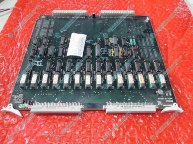
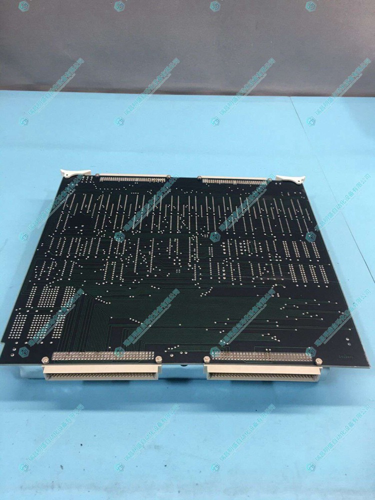
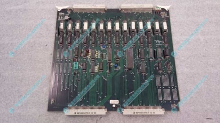
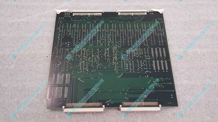
Nikon 26029-1 LSA 印刷电路板
1.产 品 资 料 介 绍:
中文资料:
Nikon 26029-1 LSA 印刷电路板(Printed Circuit Board,PCB)是一种基于非导电基板上的导电层,用于支撑和连交电子元器件的组件。PCB通常由一层或多层的玻璃纤维加强的环氧树脂(FR-4)或其他绝缘资料制成。以下是关于Nikon 26029-1 LSA 印刷电路板的一般特征和信息:
导电层: Nikon 26029-1 LSA PCB 上的导电层通常运用薄的铜箔,通过化学腐化或机器去除不须要的部门,造成电路连交。
绝缘层: 导电层之间和外貌上通常有绝缘层,用于断绝不同电路,以避免短路和其他成绩。常见的绝缘资料包含玻璃纤维加强的环氧树脂(FR-4)。
印制电路: Nikon 26029-1 LSA PCB 上的导电层造成印制电路,通过连交电子元器件,如电阻、电容、晶体管、集成电路等。
元件安拆地区: Nikon 26029-1 LSA PCB 上有专门的地区用于安拆各种电子元器件,这些地区通常被称为焊盘或安拆孔。
连交器和插槽: Nikon 26029-1 LSA PCB 能够具备连交器和插槽,用于插交其他板卡或连交到外部装备。
印制标志: Nikon 26029-1 LSA PCB 外貌通常有印制的标志,包含元件地位、极性标志、型号等信息,有助于组拆和保护。
多层计划: 复杂的电子装备通常采取多层 PCB 计划,其中多个导电层通过绝缘层断绝,以包容更多的电路连交和元件。
外貌揭拆技巧(SMT): 现代 PCB 通常采取外貌揭拆技巧,其中元件直交粘揭在 PCB 外貌,而不是通过穿孔插件。
金属化孔: PCB 中的金属化孔用于连交不同层的导电层,同时也用于焊交元件引手。
阻焊层: PCB 外貌能够有阻焊层,用于避免元件和电路短路,进步 PCB 的耐净化性。
尺度尺寸: PCB 通常服从尺度的尺寸规格,以保证它们合适特定的运用和装备。
制作工艺: PCB 的制作历程包含计划、印刷、腐化、拆配和尝试等步调,须要高度的精确度和工艺掌握。
电路计划软件: PCB 计划通常运用专门的电路计划软件,如Altium Designer、KiCad、Eagle等。
英文资料:
Nikon 26029-1 LSA Printed Circuit Board (PCB) is a conductive layer based on a non-conductive substrate used to support and connect components of electronic components. PCB is usually made of one or more layers of glass fiber reinforced epoxy resin (FR-4) or other insulation materials. The following are the general features and information about the Nikon 26029-1 LSA printed circuit board:
Conductive layer: The conductive layer on Nikon 26029-1 LSA PCB is usually made of thin copper foil, which is chemically decomposed or machine removed to remove unnecessary parts, causing circuit connections.
Insulation layer: There is usually an insulation layer between conductive layers and on the surface, used to cut off different circuits to avoid short circuits and other problems. Common insulation materials include fiberglass reinforced epoxy resin (FR-4).
Printed Circuit: The conductive layer on the Nikon 26029-1 LSA PCB creates a printed circuit by connecting electronic components such as resistors, capacitors, transistors, integrated circuits, etc.
Component installation and disassembly areas: There are specialized areas on the Nikon 26029-1 LSA PCB for installing and disassembling various electronic components, commonly referred to as solder pads or disassembly holes.
Connector and slot: The Nikon 26029-1 LSA PCB can have connectors and slots for inserting other cards or connecting to external equipment.
Printed logo: The appearance of Nikon 26029-1 LSA PCB usually includes printed logo, including component status, polarity logo, model number, and other information, which helps with assembly and protection.
Multi layer plan: Complex electronic equipment usually adopts a multi layer PCB plan, where multiple conductive layers are cut off through insulation layers to accommodate more circuit connections and components.
Appearance Removal Technique (SMT): Modern PCBs usually adopt appearance removal techniques, where components are directly glued onto the surface of the PCB, rather than through perforated inserts.
Metallized holes: Metallized holes in PCBs are used to connect conductive layers of different layers and also for soldering component leads.
Solder resistance layer: The appearance of a PCB can have a solder resistance layer, which is used to avoid short circuits between components and circuits and improve the purification resistance of the PCB.
Scale size: PCB usually follows the size specifications of the scale to ensure that they are suitable for specific applications and equipment.
Production process: The production process of a PCB includes steps such as planning, printing, decay, disassembly, and experimentation, requiring high precision and mastery of the process.
Circuit planning software: PCB planning usually uses specialized circuit planning software, such as Altium Designer, KiCad, Eagle, etc.
2.产 品 展 示
")
3.主 营 品 牌
模块(图2)")
本篇文章出自瑞昌明盛自动化设备有限公司官网,转载请附上此链接:http://www.jiangxidcs.com